S100 Computers

Home S-100 Boards History New Boards Software Boards For Sale
Forum Other Web Sites News Index    
  
An 32 MB Static RAM Board for the S-100 80386 & 80486 CPU Boards.
  
 
  32 MB Static RAM (Final)
   
  V2 32 MB RAM Board
   
  V2 32 MB RAM Board 2
   
  V3 32 MB RAM Final-2
 
Introduction
Please read up on the Master/Slave 80386 S100 board  and the 80486 S100 board before reading this page.

The 80386 & 80486 CPU boards worked fine with up to 16 MB of RAM in the S-100 bus.   The 80386 on the bus runs at 8 MHz, the 80486 up to 12 MHz.

In order to utilize the full addressing range capability (4GB) of these chips larger RAM boards are required.  Clearly the S-100 bus is not capable of meeting these addressing needs.  We solve this problem by adding, (one or more), daughter boards connected to our CPU board via two "over the top" ribbon cables.   I will call this bus the "S100-OTT bus". This provides a local data bus by which the CPU can address as much RAM as it wishes in a 32 bit wide data path and at the full CPU's clock speed.  These special RAM boards draw only power from the S-100 bus. If needed other signals could be accommodated,  but in general they are transparent to the regular S-100 bus boards.

An Early SRAM RAM Board
The first static RAM board we did was an 8MB static RAM board. The description of this board can be seen here.       
However this board still delivers far below the addressing capabilities of the 80386 CPU. 

Here is an effort to extend the addressing range to 32MB on one board.  This board utilizes 2MX8 Static RAM chips. The chips are Cypress #CY62167DV30 MoBl chips (Mouser # 727-2167DV30LL-55ZXI).  There are two issues with these chips. First they are surface mount chips, second they are expensive ($19.00 each).   In order not to end up with an expensive prototype board where the RAM chips could not be easily moved to a final "production board" Andrew came up with the idea of placing the chips on a small cassette board which is connected to the main board via a 40 pin header.  This way RAM can be easily moved from board to board.

Soldering SMT chips.   This was my first time doing large scale SMT soldering.  There are many discussions on the Web about SMT.  I found this U-Tube video helpful.  It turned out to be far easier than expected. The steps are:-

Use a very fine tip 10-15W soldering iron.  The tip must be small enough not to bridge two RAM chip pins.
With a small brush cover the board solder pads with solder paste (I use, DeoxIT Rosin Soldering Flux).
Carefully align pin one on the circuit board pad so the visible  pad is equal on both sides of the chip. (i.e. the chip is exactly centered).
Touch pin 1 with the soldering iron. If it is clean no solder is required. There is sufficient solder on the board and chip to make a connection.
Next go to pin 25. Carefully align the chip so all pins are exactly over the circuit board pads.
Solder exactly as for pin one.
Then pressing down on the chip step by step touch the end of each pin at its junction to the board.  You may feel the RAM chip getting hot. I usually stop after 5 pins for a few seconds to let things cool.
With a magnifying glass carefully examine each pin for cross bridges.  If found remove with solder wick.


After you have the board up and running remove extra flux with spray-on flux remover (3M Novec, from Mouser)
 
As with our 8 MB Static RAM board, this board is connected to the 80386 board together via two short overhead ribbon cable connectors as shown here:-
        
  32 MB Baord In the Bus
  
BTW, the ribbon cable shown here has only two boards.  This "32-Bit S-100 Overhead Bus" is designed so multiple cards can be attached to it.


RAM Board Addressing

One thing that does take a little adjusting to is the sheer range of the addressing capability of the 80386.  We will later design a DRAM S100 daughter board for this CPU, but even the current 32MB static RAM daughter board here provides a significant play area to work with.  Setting up the address line configurations requires a little care.

The CPU board itself will always address RAM on the S-100 bus if that RAM lies within the first 0-16M of the 80386's address space.  This represents the maximum capacity of the S100 buss's addressing capability.   This would require four of our 4MB S100 bus static RAM boards (and many more of many older S100 bus RAM boards).

For any RAM above 16M, the 80386 CPU board assumes it is on one or more of the daughter boards.  (BTW, the lower limit for this off S-100 bus is configurable via U13 and its input jumpers).   For our 32MB it we need to start it on a 32MB boundary so RAM will range from 2,000,000H up to 3,FFF,FFFH.  The address decoding circuit of the board is shown here:-
  
  CS Circuit
 
Laying out the address lines we have:-
A31,30,29,28,27,26,25,24,23,   22,21,20,19,18,17,16,15,14,13,12,11,10,9, 8, 7, 6, 5, 4, 3, 2, 1, 0
 
0  0  0  0  0  0  1 
0  0    x  x  x  x  x  x  x  x  x  x  x  x  x  x  x  x  x  x  x  x  x  x  x
  0  0  0  0  0  0  1 
0  1    x  x  x  x  x  x  x  x  x  x  x  x  x  x  x  x  x  x  x  x  x  x  x
  0  0  0  0  0  0  1 
1  0    x  x  x  x  x  x  x  x  x  x  x  x  x  x  x  x  x  x  x  x  x  x  x
  0  0  0  0  0  0  1 
1  1   
x  x  x  x  x  x  x  x  x  x  x  x  x  x  x  x  x  x  x  x  x  x  x
    

From the above we see that for address lines A24 & A23 and lower, the 74LS139 (a 2 line to 4 line MUX) handles the 4 banks of RAM.   Address lines A23 to A29 go directly to the 74LS682 as does one output of U14A (another 74LS139).  All switch settings on SW2 are grounded except the one to pin 7 of U20 (corresponding to A25).  This allows pin 19 of U20 to select all RAM on the board. With this configuration the range of RAM will be from 2,000,000H to 3,FFF,FFFH (32MB).  The four jumpers on P1 each select a 1 GB addressing range. Normally we will place this RAM board in the CPU's first GB range so we jumper P1, 1-2.

Study this table well. Remember address lines A2 to A22 are always within the RAM chips themselves (2M per Chip). Address lines A1 & A0 are handled by the BE0*-BE3* signals for each of the four columns of chips, so each cassette board contains 8MG.
 
There is a wait state generator on the above RAM board for slow RAM chips (U1 & jumper P23).  On this board however I am using Cypress #CY62167DV30 RAM chips which have an access time of 55ns.  Using a 32MHz clock on the CPU board I can run this board with no wait states.  This is important because it allows the 80386 to be run in "pipeline mode". This is a special mode where the CPU (with latched addressed hardware) can start "preparing" the next RAM address during its current cycle. This allows faster RAM processing overall.

However you may find if you use the board in the S-100 bus extender card with a long ribbon cable connection to the CPU in the bus you may need to add 1 or 2 wait states.

Finally,  remember because the 80386 has memory management hardware on board, you don't need contiguous RAM blocks.  It's fine to run the board with just enough RAM on the S-100 bus for say CPM-86 or MS-DOS and utilize the high speed off S-100 bus RAM for your application.

Please note. I have just noticed when using the Cyrix 80486 CPU at 40MHz with this board that its U27 needs to be a 74LS138 and not a 74F138 chip. It may be best to stick with a 74LS138 chip for all CPU's.  Currently I'm not sure if the timing issue is with the CPU board or this RAM board.  With a 74LS138 chip however all CPU's are stable -- at least up to 36MHz.

Here is a detailed breakout of the V06c mezzanine board pinouts as they relate to this board.  Note these mezzanine boards are the same ones we also use on our 16MB S100 bus RAM boards.
     
  Mezzanine Board Pinouts 32 MB Board


A V2 32/64MB S100-OTT Static RAM Board.

One thing that I did not like about the above 32/64MB static RAM boards was the use of the TTL 74LSxxx chips for decoding 8/16 bit data transfers. To get the most reliable interface with the CPU board the simpler the circuit the better. One 22V10  GAL could clearly fit the bill for a board like this.  T
his board has the following additional features:-
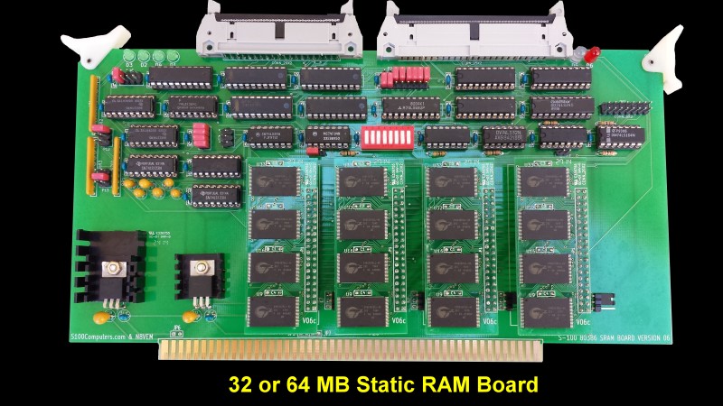
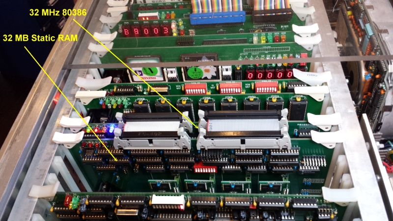
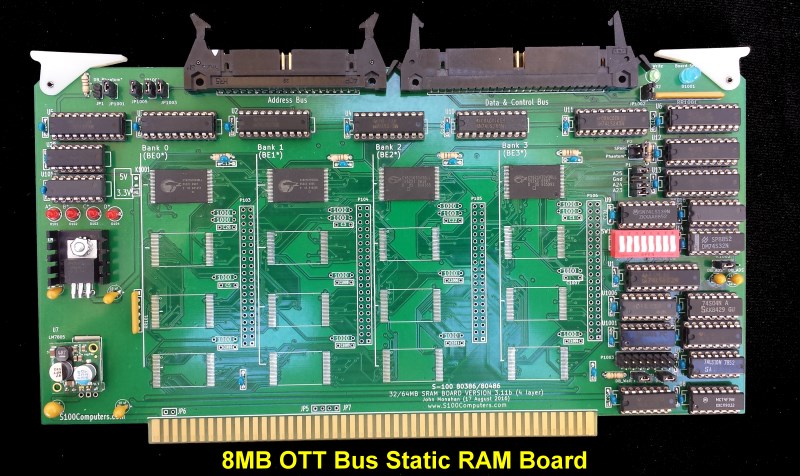
  1. I did not want to change the basic RAM board circuit. It has proven itself to be very reliable with our 80386 CPU board

  2.  I wanted to hand lay down broad power traces to all the boards IC’s for more even power distribution.

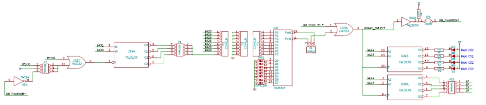
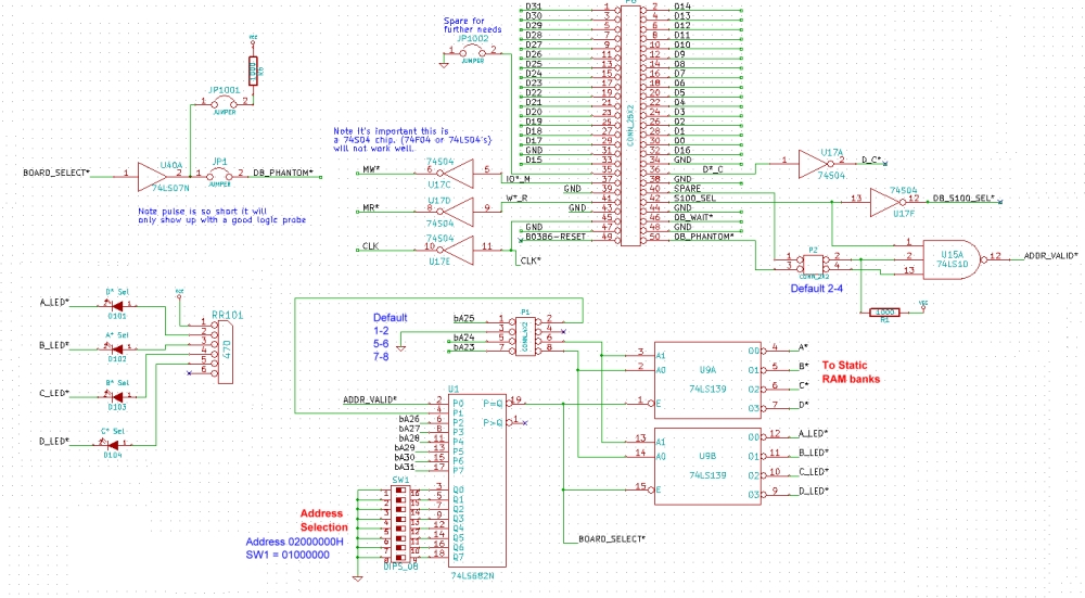
  3. This board utilizes the new RAM read and RAM write signals for memory access (see the V2 80386 board for more info). It can still be run with the earlier 80386 specific M/IO*, D/C* and W/R* which are now decoded in the onboard GAL.

  4. The one 22V10 GAL to replace a number of 74LSxx chips.  This simplifies the board and somewhat speeds up the RAM access times.  I realize not everybody is familiar with GAL’s. Please see here for more information about GALs. For those people and beginners I will supply the pre-programmed Lattice 22V10 GALs. The PALASM code is shown below.  Again these GAL’s are fairly common (Jameco #39159 for the 15ns variety).  

  5.  People should be able to simply switch IC’s from the old board to this new one. One new GAL ICs is the only major change. 

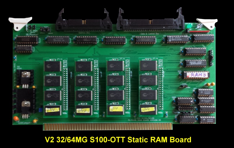
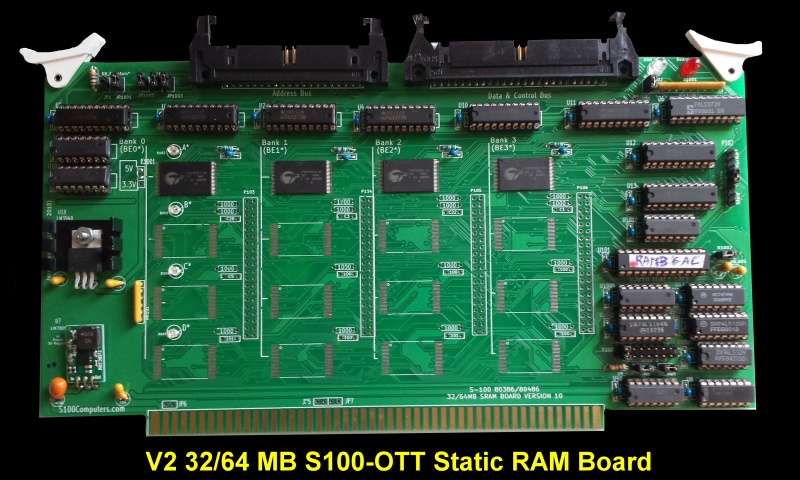
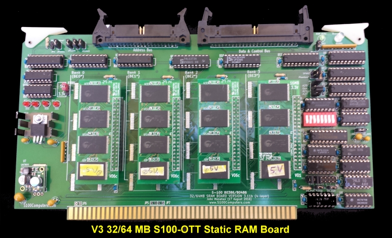
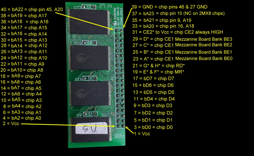
  6. The board can accommodate EITHER four Mezzanine RAM boards described above (V6.0c),  for 32MG of static RAM, or 8MB, 16MB, 24MB or 32MB by soldering the 4, 8,12,16 SMD  CY62167DV30 static RAM chips directly on the board, (or twice this capacity by soldering the newer SMD  AS6C3216 (4M X 8bit) static RAM chips on the board).

  7. I relabeled much of the Silk Screen to be more relevant. For example placing IC numbers above their pin locations etc. 

  8. Extra a long solder pads have been used to allow simpler alignment and soldering of the RAM chips to the board.    This makes soldering a lot of chips to the board tolerable.


The main difference with this board is the use of the 22V10 GAL for 32 bit data bus decoding. 
The main function of this GAL is to decode the CPU's  8 and 16 bit and 32 bit RAM Read and Write signals.
Here is the GAL22V10 relevant code:-

/BOARD_SEL@ = /A31 * /A30 * /A29 * /A28 * /A27 * /A26 * A25 * /DB_S100_SEL@ ;Will locate at 2000000H


;/MEMW@ = /CPU_M@IO * CPU_DC@ * CPU_WR@ * /BOARD_SEL@          ;For the V1 80386 Board
;/MEMR@ = /CPU_M@IO * /CPU_WR@ * /BOARD_SEL@

/MEMW@ = /EXT_RAM_WR@ * /BOARD_SEL@                            ;For the V1 80386 & 80486 Boards
/MEMR@ = /EXT_RAM_RD@ * /BOARD_SEL@

/A@ = /A24 * /A23 * /BOARD_SEL@                                 ;Top ROW of 4 RAM chips
/B@ = /A24 *  A23 * /BOARD_SEL@
/C@ =  A24 * /A23 * /BOARD_SEL@
/D@ =  A24 *  A23 * /BOARD_SEL@


Early on in the prototype stage I was concerned about the density of traces on this board.  I actually did a Mezzanine only board with wide thick traces.  I did not see any consistent difference between that board and this one that allows the use of either the mezzanine boards or direct soldering of the RAM chips to the board.

The board therefor can exist in two forms. One with 4 mezzanine boards, the other with all 16 RAM chips soldered directly to the board.  The latter is somewhat nerve wrecking.  However unlike the earlier boards and the mezzanine board the solder pads for the RAM chips are custom designed to be longer that normal. This makes soldering and chip alignment much easier. 

Be sure to carefully test the RAM board with the extensive 80386 or 80486 RAM tests.  Experienced users should have no trouble locating a faulty RAM.   Each low to high byte is arranged left to right across the board. Byte 0 on the LHS, byte 3 on the RHS.  Each 4MB block is from the top row to the bottom.

With the V2 80386 CPU board this board runs a 32MB ram test with one onboard wait state reliably using a 28MHz Oscillator.  This corresponds to a CPU CLK2 speed of 28MHz. 
Please note, we call this board here the "V2 OTT RAM board". The Silkscreen label on the board unfortunately refers to it as "32/64 SRAM Board Version 10". Sorry about the confusion


A V3 32/64MB S100-OTT Static RAM Board.
Over time I found that the above V2 OTT RAM board was somewhat "finicky" when run at high speeds for 32 bit addressing. This was particularly the case is flipping between the 80486 and 80386 CPU boards.   After many hours of testing I concluded two things were important.  For our 80486 CPU board it is absolutely essential that (U17) be a 74S04.  With this setup a 48MHz Oscillator on the 80486 CPU board works fine.  Somewhat to my surprise I found that the type and speed of the GAL U101 (a 22V10), seemed to play a large role in the reliability of the board in overnight RAM tests.  Best seem to be Lattice 15ns GAL22V10-15's (Jameco # 39159). Faster or Atmel GALs sometimes gave errors over long term tests.   After literally 100's of hours of testing and playing around I ended up with a new V3 OTT board.   I replaced the GAL completely with the following TTL circuit:-
  
  V# 32-MB RAM core Circuit
  
You can see the RAM page selection is very simple,  utilizing our tried and true 74LS682 of earlier RAM boards.  Probably more significant,  the CPU MW* (memory write) signal goes directly to each RAM chip. Note the 74S04 U17 chip.  As best I can tell this board is absolutely rock steady.  I ran it with a 48MHz Oscillator on the 80486 CPU board. No wait states on the RAM board and no delays on the 80486 board.  In the 6+ hours of  a 32MB RAM test,  never a problem.   Likewise for the 80386 CPU board.    Using a 28MHz Oscillator, corresponding to a CPU CLK2 speed of 28MHz, again 100% reliability.  However for this CPU you must add 3 wait states to the RAM board (Jumper 1003).   That's the good news, the bad news is this is a 4 layer PC board.   To get this reliability I had to use much wider traces for critical signals on this very crowded board.  While the board looks simple on the surface, underneath there are many traces branching to the numerous pins on the board.  Here again is a picture of the board:-
   
  V3 32 MB RAM board

Assembly of the board is almost identical to the V1 or V2 boards. The board can be used with the 3.3V or 5V RAM chips described above. You can use either a Pololu, EzSBC.com or old LM7805  for the 5V regulator.  Here is a picture of the board with four or the 3.3v 2M Static RAM chips soldered directly to the board.
   
  8M Static RAM
    

BUGS
/NOTES
I have not found any bugs on this board so far except that the silk screen text for P1003 should say "Wait States 1-8 "  (not 1-7).  However I do strongly advise using 74F32's and 74F245's for the RAM WR* pulses and data buffers -- particulary with the 80386.  (U28, U1011, U1006, U1016, U10, U11, U12 7 u14).

Because most S100 and S100-OTT bus signals are defined within the V2 80386 and 80486 board CPLDs there is much room to tweak both boards for higher speeds.  Indeed it is quite possible this V3 board will handle 32 bit data at the maximum rated CPU speeds. However this will mean a lower speed split for S100 bus access (or something other than a 2x, 4x, 8x.. divide of the clock in the CPLD). I have not played around with this yet. If you arrive at a different /improved CPLD code options please let me know. I will post it here.

I'm hoping this V3 board will be our definitive long term OTT RAM board for other 32 bit CPU's planned for the future. 

Rest assured there are no hardware trace errors on these boards.  If you find zeroing a region of RAM does not do so completely, if its all RAM then there is an error in the data line buffers going to the chips.  Determine which bit is stuck and follow the line. If it is only on a A0, A1, A2 or A3 (Banks 0 -3) boundary, then check solder joints to the appropriate RAM chip.  The give away here is that writing to one region of RAM will also write to another. So if you fill say 2020000-202FFFF with 0's and then fill 2000000-200FFFF with FF's, if you see FF's on every 4th byte at 2020000H then address line A21 is not soldered correctly for that chip.  Understanding exactly how these chips are addressed (on board and via the mezzanine boards) is quite tricky.  Remember for example that all S100 bus address lines to the chips are shifted up 2 address lines.  If in doubt, the simplest fix is to touch each RAM chip pin with the tip of a small pointed soldering iron tip to have the solder on the board wick up under the pin.  If you know the bank, try that one first. Take care to do so very quickly, don't let the chip get hot, best to do a few pins at a time. The 3.3 V RAMs seem particularly sensitive to overheating.


A Production S-100 Board
Realizing that a number of people might want to utilize a board like this together with a group of people on the  Google Groups S100Computers Forum, "group purchases" are made from time to time. 
Please see here for more information.


The links below will contain the most recent schematic of this board.
Note, it may change over time and some IC part or pin numbers may not correlate exactly with the text in the article above.

MOST CURRENT 32 MB STATIC RAM DAUGHTER BOARD SCHEMATIC  (V2 Final  8/18/2014)
MOST CURRENT 32 MB STATIC RAM DAUGHTER  BOARD LAYOUT  (V2 Final  8/18/2014)

MOST CURRENT 32 MB MEZZ BOARD SCHEMATIC  (V06  Final   8/182014)
MOST CURRENT 32 MB MEZZ BOARD LAYOUT  (V06   Final   8/18/2014


MOST CURRENT V2 32/64 MG RAM BOARD SCHEMATIC  (V10 FINAL, 12/28/2015)
MOST CURRENT V2 32/64 MG RAM  BOARD LAYOUT    (V10 FINAL, 12/28/2015)

Most current V2 32/64 MG RAM KiCAD files for this board   (V10 FINAL, 12/28/2015)
Most current V2 32/64 MG RAM  Gerber files for this board   (V10 FINAL, 12/28/2015)
Most current V2 32/64 MG RAM  GAL Code for this board   (V10 FINAL, 2/10/2016)
MOST CURRENT V2 32/64 MG RAM BOARD BOM List   (Rick Bromagem, 12/29/2015)

MOST CURRENT V3 32/64 MG RAM BOARD SCHEMATIC  (V11b FINAL, 12/28/2015)
MOST CURRENT V3 32/64 MG RAM  BOARD LAYOUT    (V11b FINAL, 12/28/2015)
Most current V3 32/64 MG RAM KiCAD files for this board   (V11b   FINAL, 12/28/2015)
Most current V3 32/64 MG RAM  Gerber files for this board   (V11b  FINAL, 12/28/2015)

Other pages describing my S-100 hardware and software.
Please click here to continue...

This page was last modified on 11/30/2017